1. Introduction
The integration of Printed Circuit Boards (PCBs) into moulds represents a significant advancement in smart manufacturing and the development of intelligent moulded components. By embedding electronic circuitry directly into moulded parts, manufacturers can create products that combine mechanical functionality with electronic intelligence — enabling sensing, communication, and control within a single integrated unit.
This approach is a key enabler of smart moulds, in-mould electronics (IME), and Industry 4.0 concepts.
2. Concept Overview
PCB integration in moulds involves embedding a pre-fabricated printed circuit board or flexible electronic circuitry inside the moulded component during the injection moulding or compression moulding process. The PCB may serve functions such as:
Monitoring temperature, pressure, or flow within the mould.
Controlling mould functions (e.g., valve gates, heating, or cooling).
Enabling data acquisition and wireless communication.
Providing lighting or interactive features within consumer products.
3. Integration Techniques
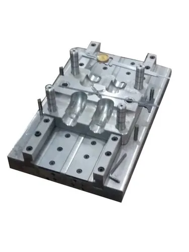
a. Insert Moulding
The PCB is placed as an insert within the mould cavity before injection.
Molten polymer is then injected around the PCB, encapsulating it within the part.
Commonly used for rigid or semi-rigid PCBs that can withstand injection pressures and temperatures.
Advantages:
Strong mechanical bond between PCB and polymer.
Suitable for high-volume production.
Challenges:
PCB must be thermally and mechanically resistant.
Careful design needed to prevent damage during injection.
b. In-Mould Electronics (IME)
Uses flexible printed electronics (polymer-based circuits) instead of rigid PCBs.
Circuits are printed or laminated on flexible films (e.g., PET or polyimide) and then thermoformed to the desired 3D shape.
The film is placed inside the mould and overmoulded with plastic.
Advantages:
Enables lightweight, thin, and complex 3D surfaces.
Ideal for touch interfaces and automotive interiors.
Challenges:
Limited current-carrying capacity.
Durability of printed conductive inks over time.
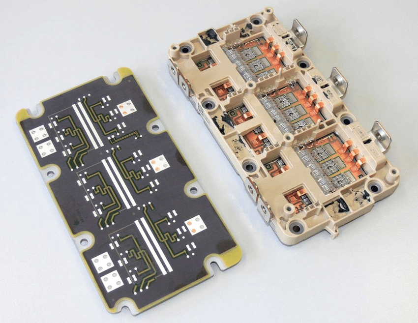
c. Overmoulding of Assembled PCBs
The PCB (possibly with components mounted) is encapsulated with a protective polymer layer through a secondary overmoulding process.
Common for sensor housings, LED modules, and medical devices.
Advantages:
Provides environmental sealing and mechanical protection.
Simplifies assembly and improves reliability.
Challenges:
Risk of heat damage to components.
Complex mould design to maintain tolerances.
4. Design Considerations
Thermal Stability: Ensure PCB materials and solder joints can withstand moulding temperatures (typically 200–300°C for injection moulding).
Mechanical Stress: Account for pressure and flow-induced stress on delicate electronic components.
Material Compatibility: Select polymers that bond well with PCB substrates and coatings.
Sealing and Insulation: Protect conductive paths from moisture and chemicals.
Accessibility: Provide access points for connectors, sensors, or wireless interfaces.
EMI Shielding: Integrate conductive layers or coatings if electromagnetic interference is a concern.
5. Applications
Automotive: Smart panels, interior controls, integrated lighting, and sensor housings.
Medical Devices: Encapsulated sensors and wearable electronics.
Consumer Electronics: Smart surfaces, touch controls, and lighting systems.
Industrial Equipment: Embedded temperature and pressure monitoring within moulds or components.
Aerospace: Lightweight, multifunctional components with integrated sensing.
6. Advantages of PCB-Mould Integration
Reduced assembly steps and wiring.
Improved reliability due to fewer connectors and solder joints.
Compact and lightweight product design.
Enhanced functionality (smart, connected components).
Better environmental protection and durability.
7. Challenges and Limitations
High tooling and process development cost.
Limited reworkability — embedded PCBs are not serviceable.
Heat management during the moulding process.
Precision alignment required for complex designs.
8. Future Trends
Printed and flexible hybrid electronics (FHE) for cost-effective integration.
Wireless power and data transfer to eliminate connectors.
Additive manufacturing combined with moulding for smart part fabrication.
Sensorized moulds for real-time process control and predictive maintenance.
9. Conclusion
PCB integration in moulds represents a transformative approach to combining electronics and mechanical structures into unified, intelligent systems. As materials, electronics miniaturization, and moulding technologies advance, this integration will enable smarter, lighter, and more reliable products across industries — paving the way for fully integrated mechatronic components and smart manufacturing ecosystems.